Explore Books on
semiconductor wafers
1-24 of 109 Books

Crystal Growth and Evaluation of Silicon for VLSI and ULSI
By Golla Eranna

On-Wafer Calibration Techniques Enabling Accurate Characterization of High-Performance Silicon Devices at the Mm-Wave Range and Beyond
By Andrej Rumiantsev

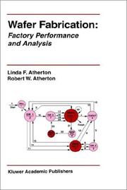
Production Planning and Control for Semiconductor Wafer Fabrication Facilities
By Lars Mönch
An automated photovoltaic system for the measurement of resistivity variations in high-resistivity circular silicon slices
An automated photovoltaic system for the measurement of resistivity variations in high-resistivity circular silicon slices
By David L. Blackburn
Handbook of Semiconductor Wafer Cleaning Technology
By Werner Kern
The invention of the silicon chip
By Windsor Chorlton
Techniques and challenges for 300 mm silicon
By Symposium F on Techniques and Challenges for 300 mm Silicon (1998 Strasbourg, France)

Cleaning technology in semiconductor device manufacturing
By
Workshop on temperature measurement of semiconductor wafers using thermocouples
Workshop on temperature measurement of semiconductor wafers using thermocouples
By Workshop on Temperature Measurement of Semiconductor Wafers Using Thermocouples (2000 NIST)
National security assessment of the U.S. semiconductor wafer processing equipment industry
National security assessment of the U.S. semiconductor wafer processing equipment industry
By United States. Dept. of Commerce. Office of Industrial Resource Administration. Strategic Analysis Division.

1996 1st International Symposium on Plasma Process-Induced Damage
By International Symposium on Plasma Process-Induced Damage (1st 1996 Santa Clara, Calif.)
1997 2nd International Symposium on Plasma Process-Induced Damage
By International Symposium on Plasma Process-Induced Damage (2nd 1997 Monterey, Calif.),Calif.) International Symposium on Plasma Process-Induced Damage (2nd : 1997 : Monterey,Kin P. Cheung,Moritaka Nakamura,Calvin T. Gabriel

Surface Characterization for Computer Disc Wafers
By John C. Stover
Ultra clean processing of silicon surfaces VII
By Paul Mertens,International Symposium on Ultra Clean P,Marc Heyns,Marc Meuris
Noise temperature measurements on wafer
Noise temperature measurements on wafer
By J. Randa
High purity silicon 9
High purity silicon 9
By International Symposium on High Purity Silicon (9th 2006 Cancún, Mexico)

Semiconductor wafer bonding
By Q.-Y Tong,U. Gösele
1999 4th International Symposium on Plasma Process-Induced Damage
By International Symposium on Plasma Process-Induced Damage (4th 1999 Monterey, Calif.)
Silicon wafer bonding technology
By Subramanian S. Iyer

Proceedings of the Fifth International Symposium on High Purity Silicon
By International Symposium on High Purity Silicon (5th 1998 Boston, Mass.)

Ultraclean surface processing of silicon wafers
By S. Heusler
Semiconductor measurement technology
Semiconductor measurement technology
By W. Murray Bullis

High-density magnetic recording and integrated magneto-optics
By James Bain